


Industry
 Num:45
 See:2217
2020-11
05
Switching power supply MOS tube loss
Switch Mode Power Supply, also known as switched Power Supply, switching converter, is a high-frequency Power conversion device, is a kind of Power Supply. Its function is to convert a potential voltage through different forms of architecture to the voltage or current required by the client. Switching power supplies convert voltages and currents between the inputs, which are mostly AC (such as mains power) or DC power, and the outputs, which are mostly devices requiring DC power, such as personal computers.
Switch losses include conduction losses and cut-off losses. Conduction loss refers to the power loss generated when the power tube is cut off to conduction. Cut-off loss refers to the power loss generated when the power tube is switched on to cut-off. Switching losses, which include turn-on Loss and turn-off Loss, are often discussed in Hard- and soft-switching. The so-called turn-on Loss refers to that when a non-ideal switching tube is turned on, the voltage of the switching tube does not immediately drop to zero, but has a time of decline. Meanwhile, its current does not immediately rise to the load current, but also has a time of rise. During this period of time, the current and voltage of the switching tube have an overlapping area, resulting in a loss, which is the switching loss. By using this analogy, we can get the cause of the turn-off loss, which will not be repeated here. Switching loss another meaning is that in the switching power supply, the parasitic capacitor needs to be charged and discharged when the large MOS tube is switched on and off, which will also cause losses.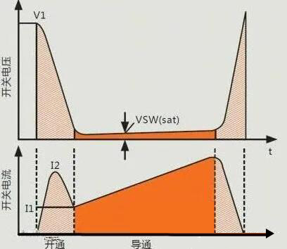
Several basic principles of MOS design and selection
1. Voltage stress
In the application of power supply circuit, the choice of drain-source voltage VDS is usually considered first. The basic principle on this is that the maximum peak voltage between the drain terminals in the actual MOSFET operating environment should not be greater than 90% of the nominal leakage source breakdown voltage in the device specification.
That is:
VDS_peak ≤ 90% * V(BR)DSS
Note: In general, V(BR)DSS has a positive temperature coefficient. Therefore, the V(BR)DSS value at the lowest operating temperature should be taken as a reference.
2. Drain current
Then consider the drain current selection. The basic principle is that the maximum periodic drain current in the actual MOSFET working environment should not be greater than 90% of the nominal maximum drain source current in the specification. The peak value of drain pulse current shall not be greater than 90% of the nominal peak value of drain pulse current in the specification, namely:
ID_max ≤ 90% * ID
ID_pulse ≤ 90% * ID P
Note: Generally, ID_max and ID_pulse have negative temperature coefficients, so the ID_max and ID_pulse values under maximum junction temperature should be taken as references. The selection of this parameter is highly uncertain -- it is mainly due to the mutual influence of working environment, heat dissipation technology, and other parameters of the device (such as conduction resistance, thermal resistance, etc.). The final decision is based on the node temperature (i.e., the "dissipated power constraint" in Article 6). As a rule of thumb, the ID in the specification will be several times larger than the actual maximum operating current in practical applications due to the limitations of dissipation power and temperature rise. In the primary calculation period, this parameter must be adjusted continuously according to the dissipation power constraint in article 6 below. ID = (3~5)*ID_max is recommended.
3. Driving requirements
MOSFEF's driving requirement is determined by its gate total charge capacity (QG) parameter. In the case of meeting other parameter requirements, try to choose QG small for the design of the drive circuit. The drive voltage is selected to keep Ron as small as possible while keeping it away from the maximum gate source voltage (VGSS) (generally using the recommended values in the device specification).
4. Loss and heat dissipation
A small Ron value is conducive to reducing the loss during the conduction period, while a small RTH value can reduce the temperature difference (under the same condition of dissipated power), so it is conducive to heat dissipation.
5. Preliminary calculation of power loss
MOSFET loss calculation mainly includes the following eight parts:
PD = Pon + Poff + Poff_on + Pon_off + Pds + Pgs+Pd_f+Pd_recover
The detailed calculation formula shall be determined according to the specific circuit and working conditions. For example, in synchronous rectifier applications, the loss during the forward guide of the internal diode and the reverse recovery loss at the turn cut-off are also taken into account. The loss calculation can be referred to in the "8 Components of MOS Tube Losses" section below.
6. Dissipation power constraint
Device steady-state loss power PD, Max should be considered based on the maximum operating junction temperature limit of the device. If the operating environment temperature of the device can be known in advance, the maximum dissipated power can be estimated by the following method:
PD, Max ≤ (Tj, max-tamb)/R j-a
R j-A is the total thermal resistance between the node of the device and its working environment, including R junpion-case,R case-sink,R sink-Ambiance, etc. If there are insulating materials, thermal resistance shall also be taken into account.
MOS tube loss of 8 components
In the process of device design selection, it is necessary to carry out advance calculation for MOSFET working process loss (the so-called advance calculation refers to the theoretical approximate calculation using the parameters provided in the device specification and the calculated value and expected waveform of the working circuit, in the case of failing to test each working waveform).
1. Conduction loss Pon
On loss is the loss caused by the voltage drop of the load current IDS(on)(t) on the on resistance RDS(on) after MOSFET is fully switched on.
Calculation of conduction loss:
First, the function expression of IDS(on)(t) is calculated and the effective value of IDS(on) RMS is calculated. Then, the resistance loss is calculated as follows:
Pon=IDS(on) RMS2 × RDS(on) × K × Don
Description:
The period used to calculate IDS(on) RMS is only the lead time Ton, not the entire work cycle Ts; RDS(on) varies with IDS(on)(t) values and device node temperatures, and the principle here is to look for RDS(on) values as close to the expected operating conditions as possible according to the specification (that is, multiplied by a temperature coefficient K provided by the specification).
2. Cut-off loss Poff
Cut-off loss refers to the loss caused by leakage current IDSS generated under the leak-source voltage VDS(OFF) stress after MOSFET is completely cut-off.
Cut-off loss calculation:
Firstly, the leakage source voltage VDS(OFF) sustained by MOSFET is calculated. Then, the IDSS provided in the device specification is searched and calculated by the following formula:
Poff=VDS(off) × IDSS × (1-don)
Description:
IDSS varies according to VDS(off), and the value provided in the specification is a parameter in an approximate V(BR)DSS condition. If the calculated drain-source voltage VDS(off) is large enough to be close to V(BR)DSS, this value can be directly referenced; if very small, zero value is preferred, i.e., this value is ignored.
3. Opening process loss
Opening loss refers to the loss caused by the cross overlap between the decreasing drain-source voltage VDS(OFF_on)(T) and the increasing load current (i.e., drain-source current) IDS(OFF_on)(t) during MOSFET opening.
Calculation of opening process loss:
Poff_on = fs x ∫ Tx VDS (off_on) (t) * ID (off_on) (t) * dt
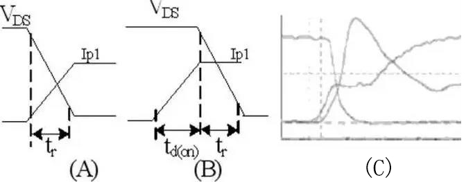
There are two main assumptions in the actual calculation -- figure (A) assumes that the initial decline of VDS(OFF_on)(t) occurs simultaneously with the gradual rise of ID(off_on)(t); Figure (B) assumes that the decline of VDS(off_on)(t) begins after ID(off_on)(t) rises to its maximum value. Figure (C) is the actual MOSFET test waveform in the FLYBACK architecture path, which is closer to the class (A) hypothesis. Two calculation formulas are extended for these two hypotheses:
Class (A) assumes Poff_on=1/6 × VDS(off_end) × Ip1 × tr × FS
Class (B) assumes Poff_on=1/2 × VDS(off_end) × Ip1 × (TD (on)+ TR) × FS
(B) Class assumptions can be calculated as values for the most egregious patterns.
Description:
In figure (C), we can see the IDS(on_beginning)>>Ip1 after starting (the Ip1 parameter in power supply is usually the initial value of excitation current). The exact value of the superimposed current crest is difficult to predict and depends on the circuit architecture and device parameters. For example, the actual current in FLYBACK would be Itotal=Idp1+Ia+Ib (Ia is the current value of the reverse recovery of the secondary rectifier diodes that the influenza should return to the primary electrode -- that is, multiplied by the turn ratio, Ib is the current released by the parasitic capacitance between the layers of the primary side winding of the transformer as soon as the MOSFET switch is turned on). This hard to predict value is also one of the main reasons for this part of the calculation error.
4. Loss during turn-off
Turn-off loss. Refers to the loss caused by the crossover overlap between the gradually rising drain source voltage VDS(on_off) (T) and the gradually falling drain source current IDS(ON_off)(t) during MOSFET switching.
(2) Resonance circuit
The circuit only changes the instantaneous current waveform of the switch and does not change the current waveform of the conduction time. As long as the appropriate L and C are selected and combined with diode junction capacitance and transformer leakage inductance, the switching tube can be switched on or off when the voltage is 0. Therefore, using resonance technology can make the switch loss is small.
(3) Soft switch technology
This circuit is in the full - bridge inverter circuit to add capacitance and diode. The diode plays a clamping role in the switching tube conduction, and forms a discharging circuit, discharging the current. Capacitance under the action of flyback voltage, the capacitor is charged, the voltage cannot be suddenly increased, when the voltage is relatively high, the current has been 0.

Switch losses include conduction losses and cut-off losses. Conduction loss refers to the power loss generated when the power tube is cut off to conduction. Cut-off loss refers to the power loss generated when the power tube is switched on to cut-off. Switching losses, which include turn-on Loss and turn-off Loss, are often discussed in Hard- and soft-switching. The so-called turn-on Loss refers to that when a non-ideal switching tube is turned on, the voltage of the switching tube does not immediately drop to zero, but has a time of decline. Meanwhile, its current does not immediately rise to the load current, but also has a time of rise. During this period of time, the current and voltage of the switching tube have an overlapping area, resulting in a loss, which is the switching loss. By using this analogy, we can get the cause of the turn-off loss, which will not be repeated here. Switching loss another meaning is that in the switching power supply, the parasitic capacitor needs to be charged and discharged when the large MOS tube is switched on and off, which will also cause losses.
Several basic principles of MOS design and selection
1. Voltage stress
In the application of power supply circuit, the choice of drain-source voltage VDS is usually considered first. The basic principle on this is that the maximum peak voltage between the drain terminals in the actual MOSFET operating environment should not be greater than 90% of the nominal leakage source breakdown voltage in the device specification.
That is:
VDS_peak ≤ 90% * V(BR)DSS
Note: In general, V(BR)DSS has a positive temperature coefficient. Therefore, the V(BR)DSS value at the lowest operating temperature should be taken as a reference.
2. Drain current
Then consider the drain current selection. The basic principle is that the maximum periodic drain current in the actual MOSFET working environment should not be greater than 90% of the nominal maximum drain source current in the specification. The peak value of drain pulse current shall not be greater than 90% of the nominal peak value of drain pulse current in the specification, namely:
ID_max ≤ 90% * ID
ID_pulse ≤ 90% * ID P
Note: Generally, ID_max and ID_pulse have negative temperature coefficients, so the ID_max and ID_pulse values under maximum junction temperature should be taken as references. The selection of this parameter is highly uncertain -- it is mainly due to the mutual influence of working environment, heat dissipation technology, and other parameters of the device (such as conduction resistance, thermal resistance, etc.). The final decision is based on the node temperature (i.e., the "dissipated power constraint" in Article 6). As a rule of thumb, the ID in the specification will be several times larger than the actual maximum operating current in practical applications due to the limitations of dissipation power and temperature rise. In the primary calculation period, this parameter must be adjusted continuously according to the dissipation power constraint in article 6 below. ID = (3~5)*ID_max is recommended.
3. Driving requirements
MOSFEF's driving requirement is determined by its gate total charge capacity (QG) parameter. In the case of meeting other parameter requirements, try to choose QG small for the design of the drive circuit. The drive voltage is selected to keep Ron as small as possible while keeping it away from the maximum gate source voltage (VGSS) (generally using the recommended values in the device specification).
4. Loss and heat dissipation
A small Ron value is conducive to reducing the loss during the conduction period, while a small RTH value can reduce the temperature difference (under the same condition of dissipated power), so it is conducive to heat dissipation.
5. Preliminary calculation of power loss
MOSFET loss calculation mainly includes the following eight parts:
PD = Pon + Poff + Poff_on + Pon_off + Pds + Pgs+Pd_f+Pd_recover
The detailed calculation formula shall be determined according to the specific circuit and working conditions. For example, in synchronous rectifier applications, the loss during the forward guide of the internal diode and the reverse recovery loss at the turn cut-off are also taken into account. The loss calculation can be referred to in the "8 Components of MOS Tube Losses" section below.
6. Dissipation power constraint
Device steady-state loss power PD, Max should be considered based on the maximum operating junction temperature limit of the device. If the operating environment temperature of the device can be known in advance, the maximum dissipated power can be estimated by the following method:
PD, Max ≤ (Tj, max-tamb)/R j-a
R j-A is the total thermal resistance between the node of the device and its working environment, including R junpion-case,R case-sink,R sink-Ambiance, etc. If there are insulating materials, thermal resistance shall also be taken into account.
MOS tube loss of 8 components
In the process of device design selection, it is necessary to carry out advance calculation for MOSFET working process loss (the so-called advance calculation refers to the theoretical approximate calculation using the parameters provided in the device specification and the calculated value and expected waveform of the working circuit, in the case of failing to test each working waveform).
1. Conduction loss Pon
On loss is the loss caused by the voltage drop of the load current IDS(on)(t) on the on resistance RDS(on) after MOSFET is fully switched on.
Calculation of conduction loss:
First, the function expression of IDS(on)(t) is calculated and the effective value of IDS(on) RMS is calculated. Then, the resistance loss is calculated as follows:
Pon=IDS(on) RMS2 × RDS(on) × K × Don
Description:
The period used to calculate IDS(on) RMS is only the lead time Ton, not the entire work cycle Ts; RDS(on) varies with IDS(on)(t) values and device node temperatures, and the principle here is to look for RDS(on) values as close to the expected operating conditions as possible according to the specification (that is, multiplied by a temperature coefficient K provided by the specification).
2. Cut-off loss Poff
Cut-off loss refers to the loss caused by leakage current IDSS generated under the leak-source voltage VDS(OFF) stress after MOSFET is completely cut-off.
Cut-off loss calculation:
Firstly, the leakage source voltage VDS(OFF) sustained by MOSFET is calculated. Then, the IDSS provided in the device specification is searched and calculated by the following formula:
Poff=VDS(off) × IDSS × (1-don)
Description:
IDSS varies according to VDS(off), and the value provided in the specification is a parameter in an approximate V(BR)DSS condition. If the calculated drain-source voltage VDS(off) is large enough to be close to V(BR)DSS, this value can be directly referenced; if very small, zero value is preferred, i.e., this value is ignored.
3. Opening process loss
Opening loss refers to the loss caused by the cross overlap between the decreasing drain-source voltage VDS(OFF_on)(T) and the increasing load current (i.e., drain-source current) IDS(OFF_on)(t) during MOSFET opening.
Calculation of opening process loss:
The cross waveform of the opening process VDS(OFF_on)(t) and IDS(OFF_on)(t) is shown in the figure above. VDS(OFF_end) before the start time, IDS(on_beginning) after the start time, Ip1 diagonally, and Tx overlap time between VDS(off_on)(t) and IDS(Off_on)(t) must be calculated or expected first. Then, it can be calculated by the following formula:
Poff_on = fs x ∫ Tx VDS (off_on) (t) * ID (off_on) (t) * dt
There are two main assumptions in the actual calculation -- figure (A) assumes that the initial decline of VDS(OFF_on)(t) occurs simultaneously with the gradual rise of ID(off_on)(t); Figure (B) assumes that the decline of VDS(off_on)(t) begins after ID(off_on)(t) rises to its maximum value. Figure (C) is the actual MOSFET test waveform in the FLYBACK architecture path, which is closer to the class (A) hypothesis. Two calculation formulas are extended for these two hypotheses:
Class (A) assumes Poff_on=1/6 × VDS(off_end) × Ip1 × tr × FS
Class (B) assumes Poff_on=1/2 × VDS(off_end) × Ip1 × (TD (on)+ TR) × FS
(B) Class assumptions can be calculated as values for the most egregious patterns.
Description:
In figure (C), we can see the IDS(on_beginning)>>Ip1 after starting (the Ip1 parameter in power supply is usually the initial value of excitation current). The exact value of the superimposed current crest is difficult to predict and depends on the circuit architecture and device parameters. For example, the actual current in FLYBACK would be Itotal=Idp1+Ia+Ib (Ia is the current value of the reverse recovery of the secondary rectifier diodes that the influenza should return to the primary electrode -- that is, multiplied by the turn ratio, Ib is the current released by the parasitic capacitance between the layers of the primary side winding of the transformer as soon as the MOSFET switch is turned on). This hard to predict value is also one of the main reasons for this part of the calculation error.
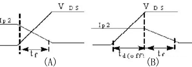
4. Loss during turn-off
Turn-off loss. Refers to the loss caused by the crossover overlap between the gradually rising drain source voltage VDS(on_off) (T) and the gradually falling drain source current IDS(ON_off)(t) during MOSFET switching.
Calculation of loss in the turn-off process:
As shown in the figure above, the loss calculation principle and method of this part are similar to Poff_on. The drain-source voltage VDS(OFF_off) and load current IDS(on_end) before the turn-off should be calculated or expected first, as shown in Ip2 and the overlap time Tx between VDS(on_off) (T) and IDS(on_off)(t). Then, it can be calculated by the following formula:
Poff_on= FS × integral of Tx VDS(on_off) (t) × IDS(on_off)(t) × dt
In the actual calculation, two calculation formulas are extended for these two hypotheses:
Class (A) assumes Poff_on=1/6 × VDS(off_beginning) × Ip2 × TF × FS
Class Poff_on=1/2 × VDS(off_beginning) × Ip2 × (TD (off)+ TF) × FS
(B) Class assumptions can be calculated as values for the most egregious patterns.
5. Drive loss Pgs
Drive loss refers to the loss caused by the gate receiving the drive power for driving
Calculation of drive loss:
After the VGS of the driving power supply is determined, it can be calculated by the following formula:
Pgs= VGS × QG × fS
instructions:
QG is the total driving power, which can be found through the device specification.
6. Dissipation loss Pds of Coss capacitance
The discharge loss of Coss capacitor refers to the discharge loss of the electric field energy stored in the MOS output capacitance Coss during the cut-off period on the drain source pole.
Calculation of dissipation losses of Coss capacitors
The VDS prior to the start time must be calculated or anticipated and then calculated using the following formula:
Pds=1/2 × VDS(off_end)2 × Coss × FS
instructions:
Coss is MOSFET output capacitance, generally equal to CDS, this value can be found through the device specification.
7. Parasitic diode forward guide loss Pd_f
The forward guide loss of the parasitic diode in MOS refers to the loss caused by the forward voltage drop when the parasitic diode in MOS carries forward current.
Forward guide loss calculation of internal parasitic diode
In some applications where a parasitic diode is used to carry current (e.g. synchronous rectification), the loss of this part needs to be calculated. The formula is as follows:
PD_f = IF × VDF × Tx × f
Where: IF is the current carried by the diode, VDF is the diode positive guide pass-pressure drop, and TX is the time of the diode carrying current within a week.
instructions:
It varies depending on the junction temperature of the device and the current carried. The value can be as close as possible in the specification book according to the actual application environment.
8. Body parasitic diode reverse recovery loss Pd_recover
Reverse recovery loss of parasitic diode in MOS refers to the loss of reverse recovery caused by reverse pressure after the parasitic diode in MOS carries forward current.
In vivo parasitic diode reverse recovery loss calculation
This loss principle and calculation method is the same as the reverse recovery loss of ordinary diode. The formula is as follows:
PD_recover=VDR × QRR × FS
Wherein: VDR is diode reverse pressure drop, QRR is diode reverse power recovery, found in the specification provided by the device.
Methods to reduce MOS tube losses
On the one hand, it is necessary to make devices with ideal switching characteristics as much as possible, and on the other hand, it is necessary to make use of new circuit technology to change the waveform of device switching period, such as transistor buffer circuit, resonant circuit, soft switch technology and so on.
(1) Transistor buffer circuit (i.e., additive absorption network technology)
The circuit technology was used in early power supply. Using this circuit, although the power loss is reduced, it is still not ideal.
- Reduce the conduction loss in the transformer behind the secondary coil with saturated inductance, add the reverse recovery time fast diode, use the characteristics of the saturated inductance to hinder the current change, limit the rate of current rise, so that the current and voltage waveform as small as possible overlap.
- Reduce the cut-off loss plus R, C absorption network, delay the transformer flyback voltage generation time, it is best to generate flyback voltage when the current is 0, at this time the power loss is 0. The circuit takes advantage of the characteristic that the capacitor voltage cannot be suddenly changed to delay the occurrence time of flyback voltage. In order to increase reliability, R and C can also be added to the power tube. However, this circuit has an obvious disadvantage: due to the presence of resistance, the absorption network loss.
(2) Resonance circuit
The circuit only changes the instantaneous current waveform of the switch and does not change the current waveform of the conduction time. As long as the appropriate L and C are selected and combined with diode junction capacitance and transformer leakage inductance, the switching tube can be switched on or off when the voltage is 0. Therefore, using resonance technology can make the switch loss is small.
(3) Soft switch technology
This circuit is in the full - bridge inverter circuit to add capacitance and diode. The diode plays a clamping role in the switching tube conduction, and forms a discharging circuit, discharging the current. Capacitance under the action of flyback voltage, the capacitor is charged, the voltage cannot be suddenly increased, when the voltage is relatively high, the current has been 0.
Share


- About
- Company Profile
- Company Honor
- Products
- FIELD EFFECT TRANSISTOR
- SCHOTTKY DIODES
- ULTRAFAST RECOVERY POWER RECTIFIER
- SIC SCHOTTKY DIODES
- Silicon carbide MOSFET
- Follow
-
Address:Room 402-404,Qianhai ChengJin Building,Moon Bay Boulevard, Nanshan District,Shenzhen
Tel:0755-88327180
Fax:0755-88327190
Email:sunny@hisemicon.com
- Contact
-
.jpg)
WeChat