


Industry
 Num:51
 See:1724
2020-11
19
MOS tube and simple CMOS logic level circuit
MOS tubes are of two types: N-type and P-type
As shown in the figure below:
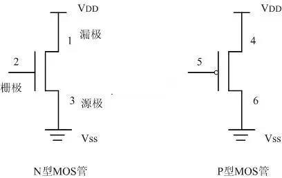
Take n-type tube as an example, and the 2 ends are the control ends, which are called "gate". The 3-terminal is usually grounded and is referred to as the "source"; The source voltage is denoted as VSS, the positive voltage at the end is called "drain", and the drain voltage is denoted as VDD. To enable terminal 1 and terminal 3 to conduct, the level on gate 2 must be increased.
For p-type tube, gate, source and drain terminals are 5 end, 4 end and 6 end respectively. To enable 4-end and 6-end conduction, gate 5 should be added to the low level.
In the logic devices made by CMOS technology or single chip microcomputer, N-type tube and P-type tube often appear in pairs. The two CMOS tubes that appear at the same time are called "complementary CMOS tubes" as long as one is on and the other is not on (i.e., "cut off" or "off") at any time.
2. CMOS logic level
The power supply voltage VDD of high-speed CMOS circuit is usually +5V. VSS grounding, it's 0V.
High level is regarded as logic "1", and the level value ranges from 65% to VDD(or VDD-1.5V to VDD).
Low levels are considered logic "0" and are required to be no more than 35% of VDD or 0 ~ 1.5V.
+1.5V ~ +3.5V should be considered as uncertain level. Uncertain levels should be avoided in hardware design.
In recent years, with the development of sub-micron technology, the power supply of single-chip microcomputer is decreasing. Low power voltage helps to reduce power consumption. CMOS devices with VDD of 3.3V have been widely used. In portable applications, VDD is 2.7V, and even 1.8V microcontroller has appeared. In the future, the supply voltage will continue to decline to 0.9V, but a level lower than 35% of VDD will be regarded as logic "0", while a level higher than 65% of VDD will be regarded as logic "1".
3.Gate
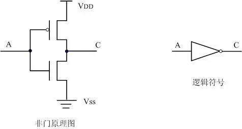
Non - gate (inverters) is the simplest gate circuit, consisting of a pair of CMOS tubes. Its working principle is as follows:
A terminal is at high level. The P-type tube is off and the N-type tube is on. The level of the output terminal C is consistent with Vss and the output is low. The A end is at low level, the P-type tube is on and the N-type tube is off. The level of the output end C is consistent with that of VDD, and the output level is high.
4. The nand gate
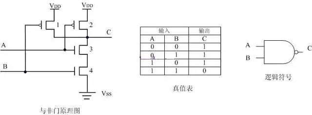
And non gate working principle:
5. Nor gate
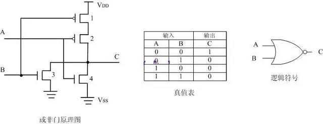
Or non-gate working principle:
Note:Remove the small circle at the output end of the above "and neither" gate and "or" gate logic symbol to become the logical symbol of "and" gate and "or" gate. The circuit diagram of realizing the function of "and", "or" must add a inverter at the output end, that is, add a pair of CMOS tubes, therefore, "and" gate is actually more complex than "and not" gate, the delay time is also longer, this point should be paid attention to in the circuit design.
6. Three states
7. Combinational logic circuit
As shown in the figure below:
Take n-type tube as an example, and the 2 ends are the control ends, which are called "gate". The 3-terminal is usually grounded and is referred to as the "source"; The source voltage is denoted as VSS, the positive voltage at the end is called "drain", and the drain voltage is denoted as VDD. To enable terminal 1 and terminal 3 to conduct, the level on gate 2 must be increased.
For p-type tube, gate, source and drain terminals are 5 end, 4 end and 6 end respectively. To enable 4-end and 6-end conduction, gate 5 should be added to the low level.
In the logic devices made by CMOS technology or single chip microcomputer, N-type tube and P-type tube often appear in pairs. The two CMOS tubes that appear at the same time are called "complementary CMOS tubes" as long as one is on and the other is not on (i.e., "cut off" or "off") at any time.
2. CMOS logic level
The power supply voltage VDD of high-speed CMOS circuit is usually +5V. VSS grounding, it's 0V.
High level is regarded as logic "1", and the level value ranges from 65% to VDD(or VDD-1.5V to VDD).
Low levels are considered logic "0" and are required to be no more than 35% of VDD or 0 ~ 1.5V.
+1.5V ~ +3.5V should be considered as uncertain level. Uncertain levels should be avoided in hardware design.
In recent years, with the development of sub-micron technology, the power supply of single-chip microcomputer is decreasing. Low power voltage helps to reduce power consumption. CMOS devices with VDD of 3.3V have been widely used. In portable applications, VDD is 2.7V, and even 1.8V microcontroller has appeared. In the future, the supply voltage will continue to decline to 0.9V, but a level lower than 35% of VDD will be regarded as logic "0", while a level higher than 65% of VDD will be regarded as logic "1".
3.Gate
Non - gate (inverters) is the simplest gate circuit, consisting of a pair of CMOS tubes. Its working principle is as follows:
A terminal is at high level. The P-type tube is off and the N-type tube is on. The level of the output terminal C is consistent with Vss and the output is low. The A end is at low level, the P-type tube is on and the N-type tube is off. The level of the output end C is consistent with that of VDD, and the output level is high.
4. The nand gate
And non gate working principle:
- A, B input are all low power, 1, 2 tube conduction, 3, 4 tube cutoff, C terminal voltage and VDD consistent, output high level.
- A input high level, B input low level at ordinary times, 1, 3 tube conduction, 2, 4 tube cutoff, C end potential and 1 tube drain to maintain the same, output high level.
- A input low level, B input high level normally, the situation is similar to, also output high level.
- A, B input are high power, 1, 2 tube cutoff, 3, 4 tube conduction, C terminal voltage and ground consistent, output low level.
5. Nor gate
Or non-gate working principle:
- A, B input are all low power, 1, 2 tube conduction, 3, 4 tube cutoff, C terminal voltage and VDD consistent, output high level.
- A input high level, B input low level, 1, 4 tube conduction, 2, 3 tube cutoff, C-end output low level.
- A input low level, B input high level, the situation is similar to, also output low level.
- A, B input are high power, 1, 2 tube cutoff, 3, 4 tube conduction, C terminal voltage and ground consistent, output low level.
Note:Remove the small circle at the output end of the above "and neither" gate and "or" gate logic symbol to become the logical symbol of "and" gate and "or" gate. The circuit diagram of realizing the function of "and", "or" must add a inverter at the output end, that is, add a pair of CMOS tubes, therefore, "and" gate is actually more complex than "and not" gate, the delay time is also longer, this point should be paid attention to in the circuit design.
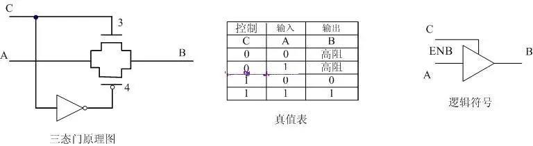
6. Three states
Working principle of tri-State gate:
When the control end C is "1", the n-type tube 3 conducts. At the same time, the level of C-end becomes low after passing through the reverter, so that the P-type tube 4 conducts, and the level of input end A can reach the output end B through 3 or 4 tubes.
When the control end C is "0", the 3 and 4 tubes are all cut off, and the level of input end A cannot reach the output end B. The output end B presents A state of high resistance, which is called "high resistance state".
This device is also known as a "transport gate with a control end". Tri-state gates with a certain drive capability are also called "buffers" and have the same logical notation.
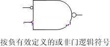
Note:It can be seen from the CMOS equivalent circuit, truth table and logical expression that by changing the position of "0" and "1", the "and not" gate becomes the "or not" gate. The signal that is valid for "1" is the "and not" relation, and the signal that is valid for "0" is the "or not" relation.
The symbols of logic devices in the above figure are the input and output relations under positive logic, that is, they are valid for "1" (high level). However, most of the control signals in MCU are defined in terms of negative validity (low level validity). For example, Chip Select signal CS(Chip Select) refers to the meaning marked by characters when the signal is "0", that is, the signal is "0", indicating that the Chip is selected. Therefore, the logical symbol of the "or not" gate can also be drawn as below.
When the control end C is "1", the n-type tube 3 conducts. At the same time, the level of C-end becomes low after passing through the reverter, so that the P-type tube 4 conducts, and the level of input end A can reach the output end B through 3 or 4 tubes.
When the control end C is "0", the 3 and 4 tubes are all cut off, and the level of input end A cannot reach the output end B. The output end B presents A state of high resistance, which is called "high resistance state".
This device is also known as a "transport gate with a control end". Tri-state gates with a certain drive capability are also called "buffers" and have the same logical notation.
Note:It can be seen from the CMOS equivalent circuit, truth table and logical expression that by changing the position of "0" and "1", the "and not" gate becomes the "or not" gate. The signal that is valid for "1" is the "and not" relation, and the signal that is valid for "0" is the "or not" relation.
The symbols of logic devices in the above figure are the input and output relations under positive logic, that is, they are valid for "1" (high level). However, most of the control signals in MCU are defined in terms of negative validity (low level validity). For example, Chip Select signal CS(Chip Select) refers to the meaning marked by characters when the signal is "0", that is, the signal is "0", indicating that the Chip is selected. Therefore, the logical symbol of the "or not" gate can also be drawn as below.
7. Combinational logic circuit
Various combinational logic circuits, such as decoder, decoder and multiplexer, can be obtained from different combinations of logic circuits, such as "and non" gate, "or non" gate, etc.
Combinational logic circuits can be implemented using off-the-shelf integrated circuits or programmable logic devices such as PAL, GAL, and so on.
Combinational logic circuits can be implemented using off-the-shelf integrated circuits or programmable logic devices such as PAL, GAL, and so on.
Share


- About
- Company Profile
- Company Honor
- Products
- FIELD EFFECT TRANSISTOR
- SCHOTTKY DIODES
- ULTRAFAST RECOVERY POWER RECTIFIER
- SIC SCHOTTKY DIODES
- Silicon carbide MOSFET
- Follow
-
Address:Room 402-404,Qianhai ChengJin Building,Moon Bay Boulevard, Nanshan District,Shenzhen
Tel:0755-88327180
Fax:0755-88327190
Email:sunny@hisemicon.com
- Contact
-
.jpg)
WeChat