


Industry
 Num:59
 See:1763
2021-02
03
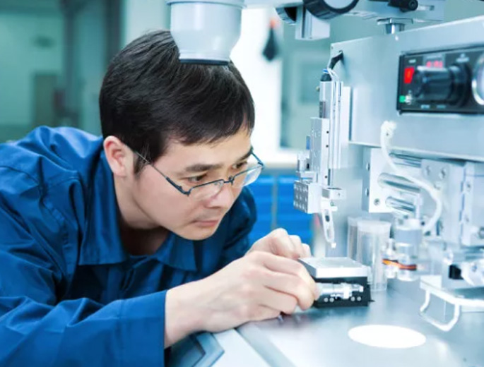
Semiconductor sealing and testing boom, advanced packaging demand is strong
Semiconductor sealing and testing include two links, packaging technology from traditional packaging to advanced packaging development.
At present, the packaging technology is gradually evolving from the traditional lead frame and lead bonding to the flip chip (FC), silicon through hole (TSV), embedded packaging (ED), fan-in/fan-out type wafer level packaging, system level packaging (SIP) and other advanced packaging technologies. Chip sizes continue to shrink, the number of pins increases, and the degree of integration continues to improve.
At present, the packaging technology is gradually evolving from the traditional lead frame and lead bonding to the flip chip (FC), silicon through hole (TSV), embedded packaging (ED), fan-in/fan-out type wafer level packaging, system level packaging (SIP) and other advanced packaging technologies. Chip sizes continue to shrink, the number of pins increases, and the degree of integration continues to improve.
Semiconductor sealing and testing boom, advanced packaging demand is strong.
Rapid growth in demand for new applications, semiconductor industry ushered in a boom recovery. In addition to the current consumer electronics, the future development of artificial intelligence (AI), 5G, Internet of Things (IoT) and other industrial applications will bring unprecedented new space to the semiconductor industry, and the global semiconductor industry is expected to usher in a new round of boom cycle.
- With Moore's Law approaching its limits, advanced packaging is expected to become a new market driver. A slowdown in Moore's Law; And driven by mega trends such as transportation, 5G, consumer, storage and computing, Internet of Things, artificial intelligence (AI) and high performance computing (HPC), advanced packaging has gradually entered its most successful period.
- China's wafer fab construction ushered in a peak, driving the direct demand for sealing and testing. According to SEMI, there will be 18 semiconductor projects under construction, up from 15 this year. China will account for 11 of these projects, with a total investment of US $24 billion. With the release of a large number of new fabs, there is more demand for semiconductor sealing and testing.
- Semiconductor foundry enterprise capacity utilization rate, sealing and testing industry is expected to welcome the new boom cycle. The capacity utilization rate of the two major domestic OEMs, SMIC and Huahong Semiconductor, has improved significantly, and the improvement of the revenue and capacity utilization rate of the OEMs will drive the development of their downstream testing manufacturers. At the same time, domestic Changdian Science and Technology, Huatian Science and Technology, Tongfu Micro Power three major sealing and testing factory revenue in the third quarter compared with the same period, the data is obviously better, China's sealing and testing industry will usher in a new boom cycle.

The global scale of closed testing has reached 56 billion US dollars, and China's closed testing market is growing rapidly.
The global semiconductor closed-test market reached $56 billion in 2018, up 5.10% year on year. ASE ranks first with 18.90% of the market share, the United States and China Changjiang Technology with 15.60% and 13.10% of the market share second and third. In addition, the top ten sealed test manufacturers, also include China's Tongfu Micro Power, Huatian Technology. In 2018, China's sealed testing market reached 219.340 billion yuan, with a year-on-year growth of 16.10%, and IC sealed testing enterprises also increased from 85 in 2014 to 99 in 2018.
China's sealed testing industry has strong competitiveness in the world. With the growth of 5G, AI, IoT and other new applications, the demand for sealed testing continues to increase, especially the demand for advanced packaging will grow rapidly. Sealing and testing three strong: Changdian Technology, Huatian Technology, Tongfu Micro Power; Jingfang Technology Co., Ltd., which mainly seals and tests cameras and sensors; Huanxu Electronics features SIP encapsulation.

Share


- About
- Company Profile
- Company Honor
- Products
- FIELD EFFECT TRANSISTOR
- SCHOTTKY DIODES
- ULTRAFAST RECOVERY POWER RECTIFIER
- SIC SCHOTTKY DIODES
- Silicon carbide MOSFET
- Follow
-
Address:Room 402-404,Qianhai ChengJin Building,Moon Bay Boulevard, Nanshan District,Shenzhen
Tel:0755-88327180
Fax:0755-88327190
Email:sunny@hisemicon.com
- Contact
-
.jpg)
WeChat