


 Num:79
 See:7208
There are mainly two kinds of structure of unit unit in SiC power MOSFET: plane structure and groove structure.
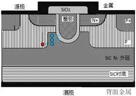
The structure of the planar SiC MOSFET, as shown in figure 1.
This structure is characterized by simple process, good unit consistency and high avalanche energy.
However, in the middle of this structure, the N region is sandwiched between two P regions, and when the current is limited to the narrow N region near the P body, the JFET effect will be produced, thus increasing the on-state resistance. at the same time, the parasitic capacitance of this structure is also larger.
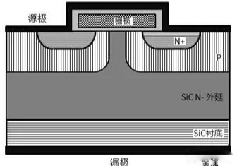
Figure 1: the structure of a planar SiC MOSFET.
The structure of the slot SiC MOSFET, as shown in figure 2.
In this structure, the gate is embedded in the matrix to form a vertical channel. Due to the trenching, the process becomes complex, and the consistency of the element and the avalanche energy are worse than the plane structure.
However, because this structure can increase the cell density, there is no JFET effect, the channel crystal plane achieves the best channel mobility, and the on-resistance is obviously lower than that of the planar structure; at the same time, the parasitic capacitance is smaller, the switching speed is faster, and the switching loss is very low, so this structure is studied and adopted in the new generation of structures.
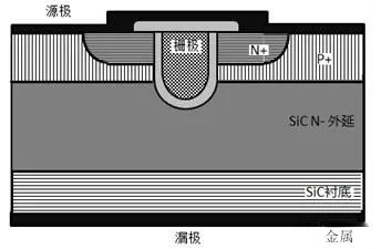
Figure 2: structure of trench SiC MOSFET.
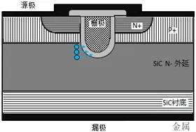
The main problem of the groove structure SiC MOSFET is that because the device works in the high voltage state, the internal working electric field strength is high, especially at the bottom of the groove, the working electric field strength is very high, and it is easy to exceed the maximum critical electric field strength locally, resulting in local breakdown and affecting the reliability of the device, as shown in figure 3.
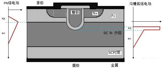
Figure 3: internal working electric field of trench SiC MOSFET structure.
Cymbal. Therefore, the technical evolution direction of the new generation of SiC MOSFET trench structure is how to reduce the working electric field intensity at the bottom of the trench, such as the double trench structure of Rohm, the asymmetric trench structure of Infineon, and so on, as shown in figure 4 and figure 5.
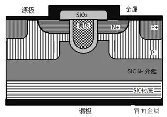
Figure 4:Rohm double trench structure
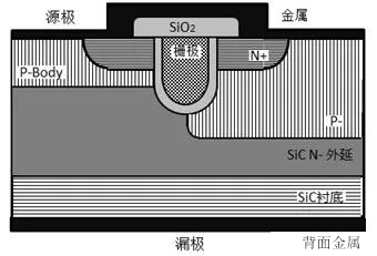
Figure 5:Infineon asymmetric trench structure.
The core of these structures is to either add a buffer layer at the bottom of the groove, or move the P region down to form a depletion layer between P and N at the bottom of the groove, as shown in figures 6 and 7, so that the electric field of the oxide layer at the bottom of the groove is partially transferred to the P region depletion layer to reduce the electric field at the bottom of the groove.
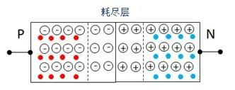
(a) the interface between P and N forms a depletion layer
(B) the electric field line under the trench
(C) Electric field lines in the lower part of the double grooves.
Figure 6: schematic diagram of reducing the working electric field at the bottom of the groove
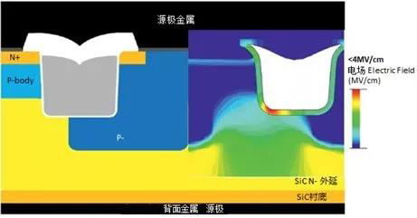
Figure 7:Infineon asymmetrical groove structure internal electric field distribution (picture source network).
The basic process and cost proportion of planar structure SiC MOSFET are shown in figure 8 and figure 9.
It can be seen that at present, the substrate of SiC crystal still accounts for a very large proportion, reaching 38%. If the substrate thinning and polishing process of SiC crystal is added, the proportion is as high as 50%.
The main reason is that SiC grows slowly, the temperature is high, the process is complex, and it is easy to produce all kinds of lattice defects.
The growth rate of Si is 100mm/ hours, the maximum diameter is 450mm, and the maximum thickness is 2m. The growth rate of sic is 100300 um/ hours, 2100 °C, the maximum diameter 150mm, the maximum thickness 50mm.
The proportion of the cost of the epitaxial process is about 17%, the proportion of the packaging cost is about 11%, and the cost caused by the yield of the product is 21%.
How to control the defects in the SiC MOSFET production process and improve the yield in the production process is still an important problem that manufacturers need to face, which is not only related to the cost of the product, but also related to the reliability of the product application in the customer.
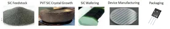
Figure 8: basic process of planar structure SiC MOSFET
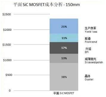
Figure 9: proportion of process cost of planar structure SiC MOSFET


- About
- Company Profile
- Company Honor
- Products
- FIELD EFFECT TRANSISTOR
- SCHOTTKY DIODES
- ULTRAFAST RECOVERY POWER RECTIFIER
- SIC SCHOTTKY DIODES
- Silicon carbide MOSFET
- Follow
-
Address:Room 402-404,Qianhai ChengJin Building,Moon Bay Boulevard, Nanshan District,Shenzhen
Tel:0755-88327180
Fax:0755-88327190
Email:sunny@hisemicon.com
- Contact
-
.jpg)
WeChat