


Industry
 Num:66
 See:1501
2021-04
26
Power Tip You Should Know: Small oversight can ruin EMI performance!
It is easy to find 100fF capacitors as parasitic elements in power supplies. Only when they are handled well can a power supply conforming to EMI standards be obtained.
The small amount of parasitic capacitance (100 mFD) from the switch node to the input lead will prevent you from meeting electromagnetic interference (EMI) requirements. So what does a 100fF capacitor look like? There are not many such capacitors in Digi-Key. Even if they do, they provide a wide tolerance due to parasitic problems.
Figure 1 is an example of one of these unplanned capacitors. On the right is a vertically mounted FET with switching nodes and clamping circuits extending to the top of the image. The input connection enters from the left and comes within 1cm of the drain connection. This is the point of failure where the switching voltage waveform of the FET can be coupled to the input bypassing the EMI filter.
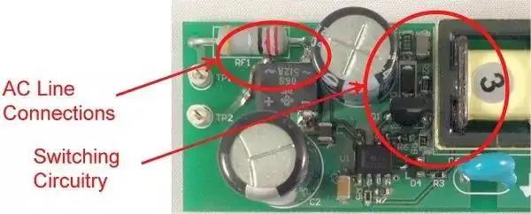
The proximity of the switch node to the input connection reduces EMI performance
Note that there is some shielding between the drain connection and the input lead provided by the input capacitor. The housing of the capacitor is connected to the main ground, providing a path for common-mode current to return to the main ground. As shown in Figure 2, this tiny capacitance can cause the EMI signature of the power supply to exceed the specification requirements.
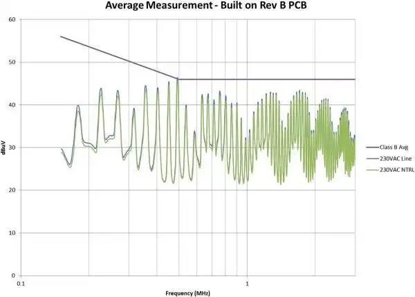
Parasitic drain capacitance results in EMI performance beyond specification requirements
This is an interesting curve because it reflects several problems: lower frequency radiation that clearly exceeds specification requirements, 1MHz to 2MHz components where common-mode problems are usually evident, and the attenuation sinusoidal (x)/x distribution of higher frequency components.
Measures need to be taken to keep the radiation within the norm. We use the general capacitance formula to reduce it:
C = ε ˙ A/d
We cannot change the permittivity (ε), and the area (A) is already minimal. However, we can change the spacing (d). As Figure 3 shows, we have increased the distance between the component and the input by a factor of three. Finally, we added shielding with a larger ground layer.
C = ε ˙ A/d
We cannot change the permittivity (ε), and the area (A) is already minimal. However, we can change the spacing (d). As Figure 3 shows, we have increased the distance between the component and the input by a factor of three. Finally, we added shielding with a larger ground layer.
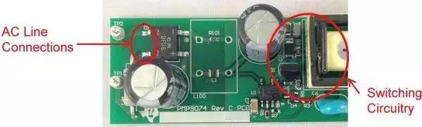
This modified layout not only increases spacing, but also provides shielding performance
Figure 4 is the modified rendering. We obtained a margin of approximately 6dB for the EMI specification at the point of failure. In addition, we have significantly reduced overall EMI signatures. All of these improvements are due only to layout adjustments, not circuit changes. If your circuit has a high voltage switch and uses a shielded distance, you need to control it very carefully.
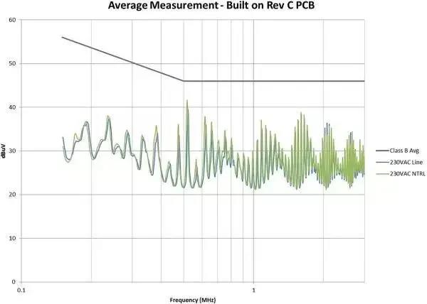
EMI performance is improved by shielding and increased spacing
In summary, a 100fF capacitor from the switch node of the off-line switching power supply can result in an EMI signature that exceeds the specification requirements. This capacity can be easily achieved with only parasitic elements, such as routing drain connections close to the input lead. This problem can usually be solved by improving spacing or shielding. To achieve greater attenuation, add filtering or slowing circuit waveforms.
Share


- About
- Company Profile
- Company Honor
- Products
- FIELD EFFECT TRANSISTOR
- SCHOTTKY DIODES
- ULTRAFAST RECOVERY POWER RECTIFIER
- SIC SCHOTTKY DIODES
- Silicon carbide MOSFET
- Follow
-
Address:Room 402-404,Qianhai ChengJin Building,Moon Bay Boulevard, Nanshan District,Shenzhen
Tel:0755-88327180
Fax:0755-88327190
Email:sunny@hisemicon.com
- Contact
-
.jpg)
WeChat